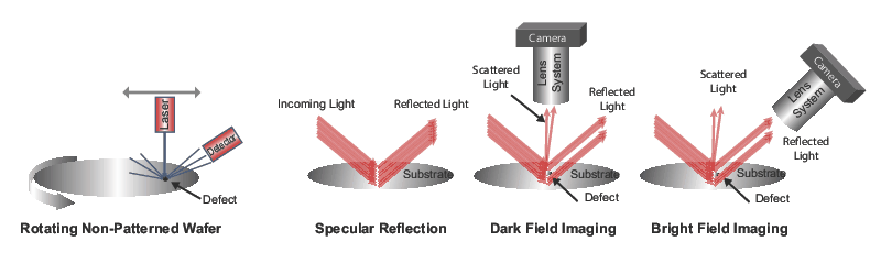
Any random defect in one of the dies will not zero out in the subtraction process showing up clearly in the subtracted image.
Patterned wafer inspection system.
Here are some of the.
The patterned wafer inspection system is able to identify defects by examining the pattern images of neighboring chips or dies and gathering the difference.
Each of these has its own features but the basic detection principles are the same.
The new inspection systems are extensions of the company s flagship patterned wafer platforms featuring advancements in the speed and sensitivity that define optical inspection.
We do not have the expertise to fully test this unit and have documented all the information gathered from it in this page.
The new e beam review system introduces innovations that cement its value as the essential link between defect and source.
Patterned wafer inspection system.
High throughput and sensitivity allow these tools to detect such process issues and to identify critical base line defects that must be corrected to improve yields.
Klac announced the revolutionary esl10 e beam patterned wafer defect inspection system the new system is designed.
Image processing software subtracts one image from the other.
In 2017 the unpatterned wafer inspection.
Milpitas calif july 20 2020 prnewswire today kla corporation nasdaq.
Klac announced the revolutionary esl10 e beam patterned wafer defect inspection system the new system is designed to accelerate time to market for high performance logic and memory chips including those that rely on extreme ultraviolet euv lithography by detecting and reporting defects that cannot be routinely captured by optical or other e beam defect.
Inspection is divided into two inspection systems a patterned wafer inspection system and a non patterned wafer inspection system.
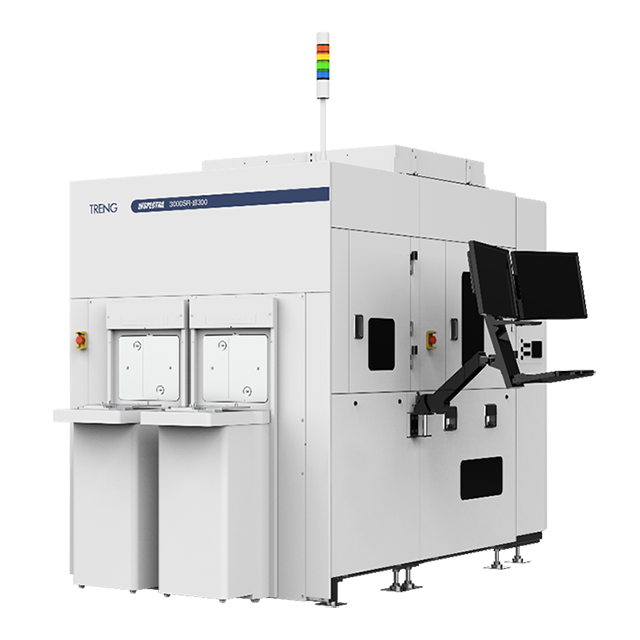
This kla tencor sfs 7600 surfscan patterned wafer inspection system is used and in good condition.
This information allows engineers to detect resolve and monitor critical yield excursions resulting in faster yield ramp and higher production yield.
Patterned and unpatterned wafer defect inspection and review systems find identify and classify particles and pattern defects on the front surface back surface and edge of the wafer.
In contrast unpatterned wafer inspection is less understood but the technology is also critical.
There are many types of patterned wafer inspection systems including the electron beam inspection systems the bright field inspection systems and the dark field inspection systems.
Unpatterned wafer inspection is used for all types of devices such as those with iii v materials analog logic and memory.
Patterned wafer inspection systems are a critical component in a fab s yield learning strategy providing in line detection of pattern defects and contaminants which drive down yields.
Patterned wafer inspection systems compare the image of a test die on the wafer with that of an adjacent die or of a golden die known to be defect free.
It is recommended that the purchaser of this system contact kla tencor for installation.