Pcb Board Design Course In Chennai

Pcb Training In Chennai In 2020 Web Design Training Online Web Design Simple Website Design

Our Training Modules Are Designed And Structured To Benefit College Pass Out Students Job Seekers S Circuit Board Circuit Board Design Electronic Engineering

Technical Workshop On Printed Circuit Board Pcb Design Circuit 2019 At Tharamani Chennai Events High

Pcb Design Course In Chennai Pcb Design Course Hiton Technologies

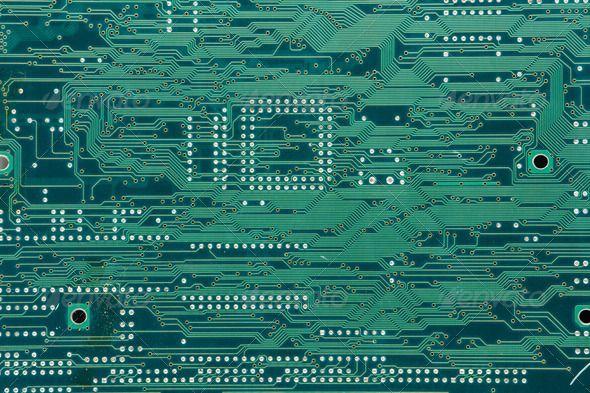
Printed Circuit Board Design In Chennai Ggg Circuits

Pcb Design Make Arduino Nano Using Altium Designer Circuit Board Design Pcb Design Printed Circuit Board
Pcb designing training computer networking training.
Pcb board design course in chennai.

Printed Circuit Board Design Workshop Pcb 2019 At Tharamani Chennai Events High

Choose Ipc A 610 Certification Program For Specialist Best Inc Printed Circuit Boards Writing Skills Circuit Board

Alltechz Solutions Ats Is The Best Pcb Training Institute In Kanchipuram Train Chennai Technology
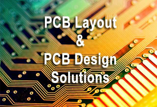
Virya Infotech Pcb Design In India Pcb Design In Chennai High Speed Pcb Design Pcb Design Services Pcb Design Training
Source : pinterest.com
